 KeltriREADER
Help center
Appearance and highlighting
Calibrate visual contrast, configure grid rulers, and customize net palettes.
Theme and canvas
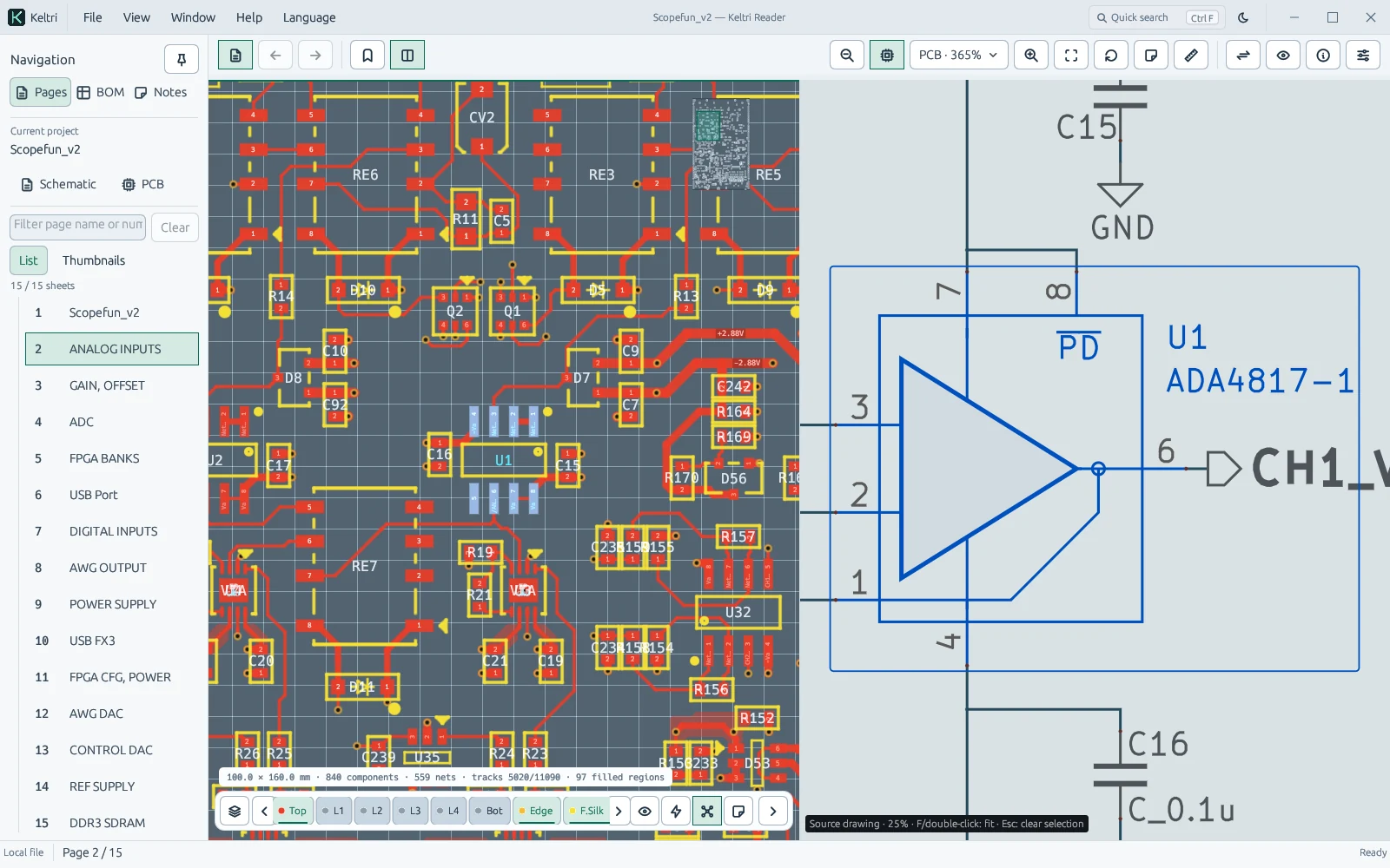
The title bar toggles between calibrated Deep Dark and Soft Light themes. The inspector provides independent background controls for the PCB substrate and schematic paper tone.
Light mode uses low-saturation engineering gray rather than blinding pure white, maintaining crisp contrast for copper traces, soldermask boundaries, and silkscreen markings.
Grid settings
PCB and schematic viewports feature independent reference grids: choose between off, orthogonal line grids, or subtle dotted matrices, with adjustable spacing and opacity.
Grids adapt dynamically across power-of-two zoom steps, providing spatial proportion cues without altering raw design coordinates or snapping targets.
Object and text visibility
In the Display → Objects tab, toggle categories independently: traces, through-holes, blind/buried vias, SMD pads, copper fills, references, values, and in-trace net badges.
When inspecting dense BGA pinouts, hiding polygon copper fills exposes underlying trace routes and decoupling connections with zero obstruction.
Highlight palettes and multiple nets
Multiple concurrent net highlights utilize high-contrast palettes: selected signals shine in vivid hues (electric cyan, coral red, amber, emerald), while unselected copper darkens gracefully.
Selecting bus groups (such as SCL/SDA or SPI channels) automatically assigns distinct complementary colors with inline badges, preventing signal confusion.