 KeltriREADER
Help center
Read a PCB
High-precision pad picking, layer isolation, X-ray perspective, and board measurements.
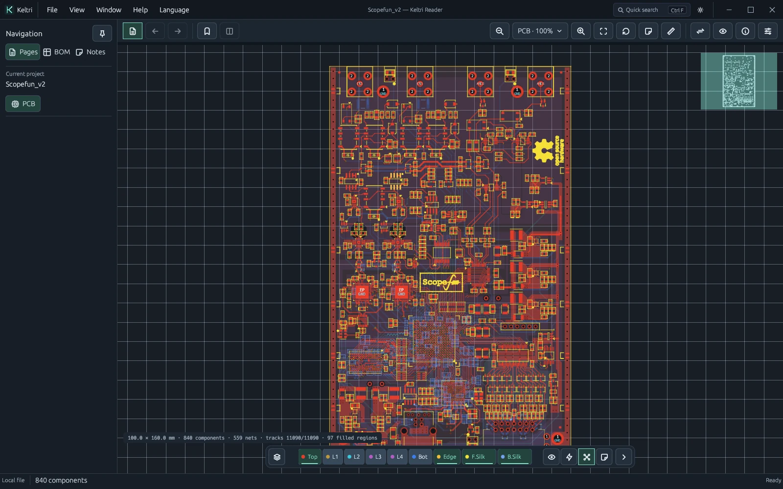
Pick a net or a component
Clicking a pad selects the pin and highlights its electrical net; Alt+click selects the parent component. When inspecting dense passives, BGA ball grids, or stacked vias, resting the cursor summons a hover card showing reference and net data.
If geometry overlaps densely, keep the cursor in place and tap Tab to cycle through candidates sequentially, eliminating pick ambiguity in tight layouts.
Three layer states
Press L to toggle the floating layer dock. Each layer button cycles through three states: active isolated, locked visible, and hidden. In single-layer isolation, non-active copper fades away, making dense trace paths effortless to follow.
Tap + or - on the numeric keypad to step through physical layers in stackup order (from Top Layer through internal planes to Bottom Layer) without taking your hand off the mouse.
Multi-net, X-ray and measurement
Press X to engage X-ray multi-layer perspective: the selected net cuts through all copper layers as a glowing skeletal trace, highlighting interlayer vias with crisp white rings.
Press R to toggle Prim-algorithm ratline vectors between unrouted pads. Press M to activate the measurement ruler, which measures point-to-point distances, orthogonal deltas, and trace widths for physical bring-up.